- Synthetic DNA Enables Precise Nanoscale Architecture for Advanced Memory Devices
- The device operates using less than one-tenth of standard voltage levels.
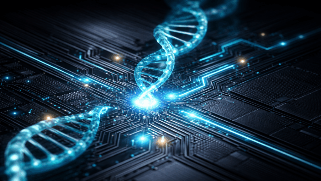
- DNA and perovskite combination creates highly efficient conducting channels
A Penn State research team has developed a new type of memory device that combines synthetic DNA with perovskite semiconductors to achieve high storage density using very little energy.
The device, known as a memristor, can remember the direction of previous current flow even after its power supply is turned off.
This ability to store and process data in the same location mimics how neurons in the brain work, potentially allowing for more efficient data processing.
Article continues below.
How DNA and perovskite work together in the device
The team applied silver nanoparticles to custom synthetic DNA sequences and integrated them with crystalline perovskite thin films.
This process, called doping, made DNA capable of conducting electricity and at the same time directing its units in a more agile way.
Unlike natural DNA, which behaves like long, intertwined strands of wet spaghetti, short, rigid fragments of synthetic DNA enable true architectural precision at the nanoscale.
“We can computationally determine exactly what sequences we need and what length they should be, and then we can rationally design them with synthetic DNA,” said co-author Neela H. Yennawar.
The DNA and perovskite together developed biohybrid channels that channel current flow through the device.
When the team applied less than 0.1 volts, compared to 120 volts from a standard U.S. outlet, electrons moved reliably through the system.
The device performed the same memory functions as existing technologies, but consumed only a tenth of the energy, making it much more suitable for low-power electronics.
It also ran consistently at temperatures up to nearly 250 degrees Fahrenheit and remained stable at room temperature for more than six weeks.
With these results, it far exceeds the performance standards of current perovskite-based memory storage devices.
“Using just DNA or just perovskite didn’t produce as strong a result as the combination,” said Kavya Keremane.
“It is this combination that enables very high memory storage density that requires very little power.”
DNA is nature’s most efficient storage mechanism, capable of storing around 215 million GB of data per gram.
“Nature has the solution; we just have to find it and apply it,” said researcher Bed Poudel.
“This work of integrating DNA into electronics to do amazing things gives a glimpse of what is possible.”
Applying that capability to electronics could enable more efficient data centers, faster data processing, and the ability to process much more complicated data.
The researchers have filed a patent application and plan to refine their approach while investigating other bioinspired electronics applications.
Through Storage bulletin
Follow TechRadar on Google News and add us as a preferred source to receive news, reviews and opinions from our experts in your feeds.