- Fotonic chips with quantum lasers are finally being built without redesign the entire system
- These lasers work directly in silicon and still survive the great heat for more than six years.
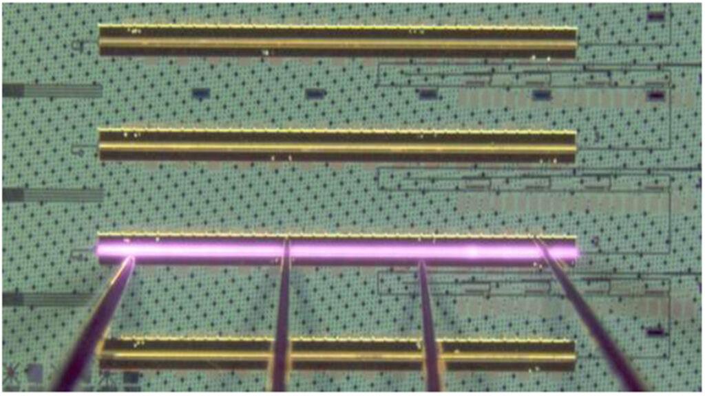
- The researchers from the University of California filled the laser gap with polymers and the precision beam control nailed to the chip
A new manufacturing method could cause photonic circuits to be cheaper and more practical directly integrating the quantum spot (QD) in silicon chips, a process that could influence how future domestic devices, physical conditioning trackers and portable computers are designed.
The research team, led by Rosalyn Koscica at the University of California, achieved this by combining three key strategies.
They used a pocket laser configuration for direct integration, followed a two -step growth method that involves deposition of metalorganic chemical steam and molecular beam epitaxia, and introduced a polymer gap filling technique to reduce the propagation of the optical beam.
Close the gap with careful engineering
This development addresses long -standing challenges that involve material incompatibilities and coupling inefficiencies that historically have limited the performance and scalability of integrated photonic systems.
Combined efforts minimized the initial interface gap and made it possible for the lasers to reliably work in silicon fotonic chiplets.
As the researchers point out, “Fotonic Integrated Circuit Applications (PIC) require chip light sources with a small device footprint to allow the integration of densest components.”
The new approach allows a stable laser in the band frequency or, which is suitable for data communications in data centers and cloud storage systems.
When integrating the lasers directly with ring resonators made of silicon or using Bragg reflectors distributed from silicon nitruro, the team has also addressed problems related to alignment and optical feedback.
One of the most surprising findings of the investigation is how well the low heat works.
“Our integrated QD lasers demonstrated a high temperature temperature of up to 105 ° C and a useful life of 6.2 while operating at a temperature of 35 ° C,” says Mrs. Koscic.
These performance metrics suggest a thermal stability level previously difficult to achieve with integrated monolithically designs.
This thermal resilience opens the door to more durable applications in real world environments, where temperature fluctuations can limit the reliability of photonic components.
It can also reduce the need for active cooling, which has traditionally added costs and complexity to past designs.
Beyond performance, the integration method seems appropriate for large -scale manufacturing.
Because the technique can be executed in standard semiconductor foundations and does not require important changes in the underlying chips architecture, it is promising for broader adoption.
The researchers argue that the method is “profitable” and “can work for a range of integrated photonic chips designs without the need for extensive or complex modifications.”
That said, the approach will probably face scrutiny regarding the consistency in large wafers and compatibility with commercial photonic systems.
In addition, success in controlled laboratory environments does not guarantee a perfect implementation in mass manufacturing configuration.
Even so, the combination of a compact laser design, compatibility with conventional processes and the integration of the band functionality or make this development notable.
From data centers to advanced sensors, this silicon compatible laser integration could bring photonic circuits closer to the viability of the mass market.
Via IEEE