- Sandisk recruits superior computer minds to shape the flash -based memory alternative for AI
- HBF memory backed by RISC and GPU leaders promises a high bandwidth and mass capacity
- Patterson and Koduri join Sandisk to guide the expansion of flash memory beyond the HBM limits
Sandisk has designated two main figures in computing to help shape the direction of its high capacity memory technology for AI workloads.
Professor David Patterson and Raja Koduri have joined the new Sandisk Technical Advisory Board to provide strategic and technical information about high bandwidth (HBF), an alternative based on flash to the high -width band memory (HBM).
Patterson is accredited by the development of the computer science of the reduced instructions (RISC) and the redundant variety of economic discs (RAID), and will direct the advisory board. Koduri is known for his leadership in graphic architecture, which has supervised GPU designs in AMD and Intel.
Decades of experience
Together, they provide decades of experience through computer science, memory systems and large -scale architecture.
“We are honored that two distinguished computer architecture experts join our Technical Advisory Board,” said Alper Ilkbahar, executive vice president and Sandisk technology director.
“Your collective experience and strategic lawyer will be fundamental to configure HBF as the future memory standard for the AI industry, and stating that we not only meet but exceed the expectations of our clients and partners.”
Patterson said: “HBF shows the promise to play an important role in the AI of the data center by offering an unprecedented memory capacity to a high bandwidth, which allows inference workloads to be far beyond today’s limitations. It could reduce the costs of new AI applications that are currently not affectable.”
Koduri added: “HBF is configured to revolutionize the EDGE by equipping devices with memory capacity and bandwidth capabilities that will admit sophisticated models that are executed locally in real time. This advance will unlock a new era of intelligent edge applications, fundamentally changing how and where the inference of AI is performed.”
HBF is designed to match the HBM bandwidth while offering up to 8 times the capacity at a similar cost.
Built with flash BICS, BICS WAFER CBA and patented stacking that allows 16 packet for package, HBF offers a new way of expanding GPU’s memory without depending completely on a expensive dram.
While it is not a direct replacement for HBM, HBF shares the same electrical interface and only requires minimum protocol changes.
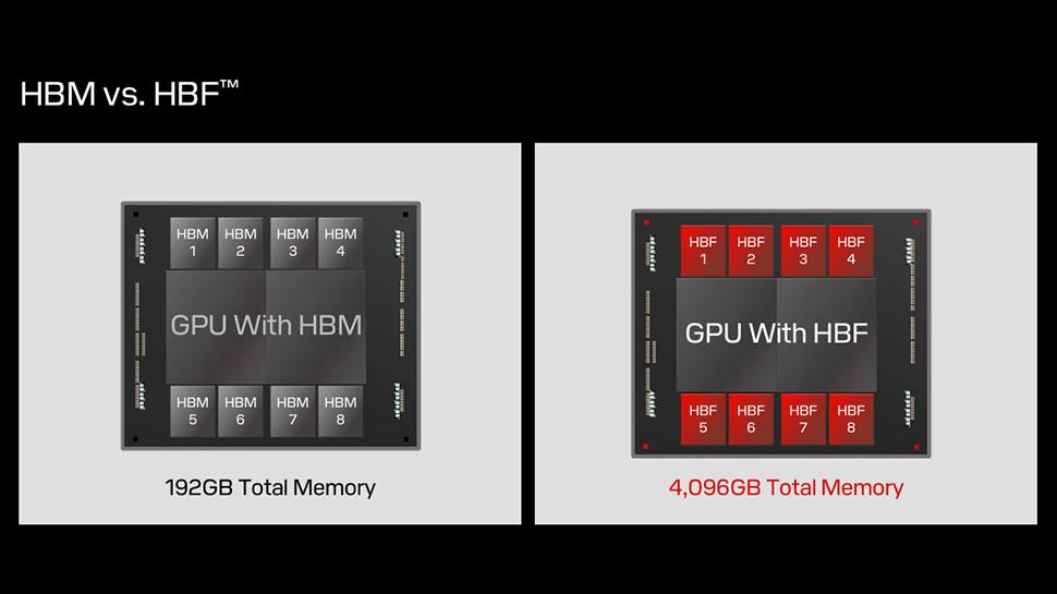
Sandisk previously demonstrated how an AI GPU that uses only HBM could admit 192 GB of memory, but when combining it with HBF, that figure could reach 3TB.
In a configuration using HBF only, the memory capacity could climb up to 4TB.
The technology was revealed for the first time in the future FWD 2025 Sandisk investor event in February 2025, along with its road map for future HBF generations.
These updates show increases in the ability and bandwidth over time, with some compensation in energy efficiency.
By forming an advisory board and looking for an open standard development, Sandisk is trying to avoid blocking the market in patented solutions.
This can help traction against rivals such as Samsung and SK Hynix, who are strongly invested in HBM space.