- IMEC researchers have found a way to grow laser directly in silicon
- IMEC lasers use Gallium arsenide, a material that does not naturally bind with silicon
- This advance could reduce costs and improve photonic chips for AI and Telecom.
Silicon Photonics uses light to transmit data instead of relying on electrical signals, but since silicon itself cannot generate light efficiently, it requires lasers as a light source.
Placing the lasers in the fries has traditionally been a challenge since silicon, a material that is commonly found in the sand, is not suitable for lasering, and the best laser materials, such as Gallium Arsenuro (GAA), no They work naturally with him. The existing methods need to unite these materials in Silicon, a process that is expensive and wasteful.
The scientists of the IMEC Belgium Research Center have presented a solution to this problem that involves the cultivation of lasers directly on silicon. This discovery could lead to more affordable and scalable photonic devices, potentially transforming applications into data communication, automatic learning and AI.
Short wavelengths
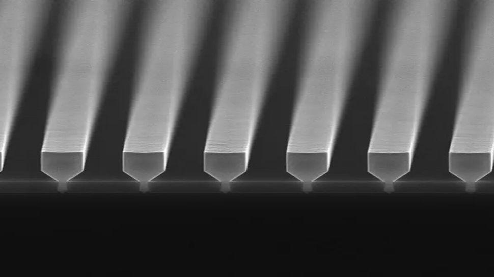
The IMEC approach, detailed in an article published in NatureIt is based on Nano-Cridge engineering, which limits the defects that would otherwise degrade laser performance.
They start covering a silicon wafer with a silicon dioxide lay IEEE Spectrum describes it). Gallium Arsenuro is deposited in these trenches, where he only makes contact with silicon at the bottom. This placement maintains buried defects inside the ditch and prevents the propagating material from being propagated.
The lasers use multiple quantum wells of Galio Indian Arsenuro (Ingaas) as an optical gain region and are integrated into a Pin -Papapping diode structure. They operate at room temperature with continuous wave electric injection, achieving threshold currents as low as 5 ma and exit powers of up to 1.75 MW.
“In recent years, IMEC has been a pioneer in Nano-Ridge Engineering, a technique based on SAG [selective-area growth] and art [aspect-ratio trapping] To grow nano-vitucios III-V of low definition outside the trenches, ”said Bernardette Kuner, IMEC scientific director.
“Now, IMEC exploded the II-V Nano-Ridge Engineering concept to demonstrate the first complete manufacturing at the scale of gaa-based laser wafers pumped into standard 300 mm silicon wafers, completely within a pilot manufacturing line of pilot manufacturing CMOS “.
Nanoridge lasers emit light at 1,020 nanometers, which IEEE Spectrum He points out, it is a shorter wavelength than those typically used in telecommunications. IMEC researchers say they are actively working to extend the wavelength and improve the design to reduce defects near electrical contacts. If it succeeds, this approach could provide a scalable and profitable solution to integrate the lasers into silicon photonics, paving the way for high performance optical devices of the future.