
- Huawei proposes the Tau Scaling Law as an alternative to stop Moore’s Law
- LogicFolding architecture reduces signal delay through vertically stacked semiconductor circuit designs
- Traditional transistor shrinkage faces increasing physical and economic limitations across the semiconductor industry
For more than five decades, the semiconductor industry has relied on a simple and powerful prediction, Moore’s Law, which states that transistors on a chip double approximately every two years, has now hit serious physical and economic walls.
The global industry faces a slowdown in geometric scaling and the steady erosion of cost-per-transistor benefits.
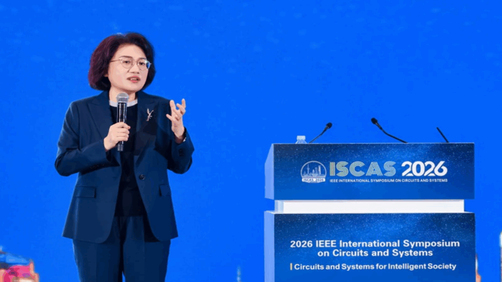
This common challenge has forced all major players to look for a new way forward, and at the 2026 IEEE International Symposium on Circuits and Systems (ISCAS), Huawei’s He Tingbo proposed an alternative framework called Tau Scaling Law (τ).

A new guiding principle for Shanghai
According to Huawei, her peers and colleagues have already dubbed this approach “Her Law” in recognition of her leadership.
Instead of focusing on reducing transistor dimensions, this principle prioritizes reducing signal propagation delay.
Huawei believes that compressing the time constant τ can drive the continued evolution of semiconductors and electronic systems.
The key technological advance enabled by this new law is a technique called LogicFolding.
Traditional chip design arranges all electronic components on a flat 2D grid that limits the closeness of circuits, and LogicFolding instead breaks the physical limits of conventional circuit designs by dramatically shortening critical path wiring.
Reduces resistive and capacitive loading that normally slows signal propagation between transistors.
The result is a systematic compression of the time constant τ at both the circuit and chip levels simultaneously.
Huawei has abandoned traditional 2D chip design in favor of a layered 3D architecture.
Think of this transition like going from a single-story house to a multi-story building with efficient elevators: Huawei can now stack multiple flat circuits vertically, creating space for more transistors while also placing the core components closer together.
Shorter transmission distances between circuits directly improve frequency and overall performance.
Practical results and future ambitions
Huawei claims that it has already mass produced 381 chips using this new scaling law in various industries.
The upcoming Kirin chips, scheduled for release in fall 2026, will be the first to adopt the LogicFolding architecture.
By 2031, the company expects its high-end designs to reach a transistor density equivalent to 14 Å or 1.4 nm processes.
“We believe that openness and collaboration are key to driving continued progress in the semiconductor industry,” said He Tingbo.
“No company can independently find all the answers on the path of semiconductor evolution.”
Huawei has every incentive to project confidence, given its current restrictions on accessing advanced manufacturing tools from TSMC or purchasing Nvidia’s latest AI chips.
It remains an open question whether the τ Scaling Law can actually outperform Moore’s Law over the next decade.
Competing companies are likely to treat this announcement with moderate skepticism until real hardware reaches neutral testing labs.

Follow TechRadar on Google News and add us as a preferred source to receive news, reviews and opinions from our experts in your feeds.