- ZAM stacks nine layers of working memory vertically within each compact module
- Each ZAM memory layer reportedly contains exactly 1,125 GB of DRAM capacity
- ZAM’s estimated bandwidth numbers are now very close to Nvidia HBM4 performance territory
Computer memory architecture will undergo a significant structural transformation in the coming years.
A new design called Zero Angle Memory (ZAM) stacks chips vertically rather than spreading them out on a flat surface, a change that could increase data transfer speeds while reducing power consumption.
Intel has supported this technology as a possible replacement for existing HBM memory.
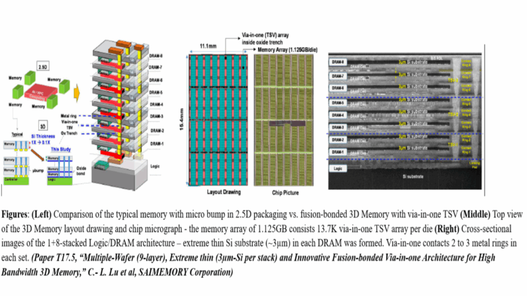
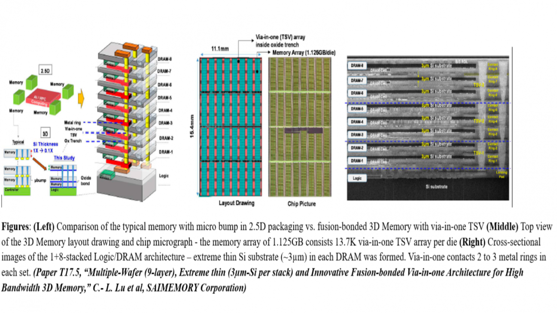
Inside the nine-layer ZAM memory design
Technical diagrams from an upcoming VLSI conference paper have now revealed the internal details of this memory design.
Eight separate DRAM storage layers sit beneath a single control layer within each ZAM module built by the consortium.
This arrangement provides each module with a total of nine functional layers stacked on top of each other vertically.
Images from the conference paper show how each of the eight DRAM layers contains exactly 1,125 GB of storage capacity.
Therefore, basic math offers approximately 9 GB of total memory per ZAM module before any general deductions.
Three through-silicon vias (TSVs) run through the entire vertical stack to connect each layer electrically from top to bottom.
Intel developed the fusion bonding method that creates these TSV connections with extreme precision and reliability.
Each DRAM layer is separated from its neighbor by a silicon substrate just 3 microns thick.
Those TSVs connect to two or three metal rings in each layer to achieve stable electrical flow.
Bandwidth estimates derived from previous claims now put ZAM close to the performance figures of HBM4 from Nvidia’s Vera Rubin platform.
ZAM targets HBM4 class bandwidth
A Japanese company called Saimemory Corporation is leading the commercialization effort for this Intel-backed technology.
Saimemory operates as a wholly owned subsidiary of SoftBank and has not yet released official data rates for this new memory design.
Previous statements from the company suggested a two to three times speedup over current HBM3 memory standards.
HBM3 currently offers 819 GBps (or 6.4 Gbps) of bandwidth in its current standard configuration, so tripling that baseline would give ZAM about 2.5 TBps of total performance for AI processors.
Nvidia’s Vera Rubin AI platform reportedly relies on HBM4 for its highest available bandwidth configurations.
This performance parity puts Intel’s HBM memory technology in direct competition with Nvidia’s preferred memory standard.
At this time, no working ZAM prototype has yet been shown to independent reviewers or third-party testing labs anywhere in the world.
Manufacturing eight bonded layers without introducing defects remains a difficult and untested industrial challenge for this consortium.
HBM4 already benefits from Nvidia’s established production roadmap and existing global supply chains from multiple suppliers.
A memory standard with superior technical specifications often fails without broad ecosystem adoption and industry support over time.
The June VLSI conference presentation will determine whether Intel’s claims about the HBM killer move beyond paper diagrams into physical reality.
Via HPC WIRE
![]()
Follow TechRadar on Google News and add us as a preferred source to receive news, reviews and opinions from our experts in your feeds.